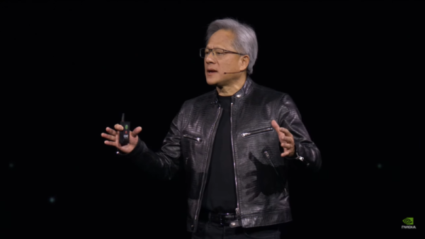
Market news pointed out that NVIDIA (NVIDIA), a large-scale graphics chip manufacturer, has started the self-designing of Base Die for high-frequency wide memory (HBM). In the future, no matter what brand of DRAM memory you need, your logical chips...
Market news pointed out that NVIDIA (NVIDIA), a large-scale graphics chip manufacturer, has started the self-designing of Base Die for high-frequency wide memory (HBM). In the future, no matter what brand of DRAM memory you need, your logical chips will adopt NVIDIA's own design solution. It is expected to be made using a 3-nanometer stage process and will start trial production as soon as the second half of 2027.
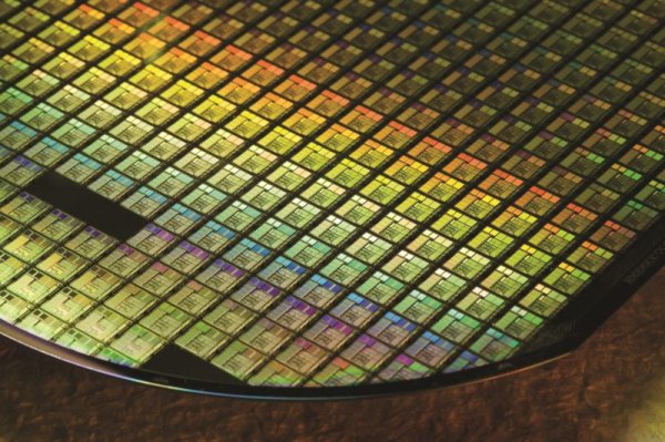
According to the report of the industrial and commercial time report, in the current HBM market, South Korea is SK Hynix is the leading manufacturer, and its HBM Base Die has adopted self-made solutions in the past. However, once the HBM transmission speed is to be increased to more than 10Gbps per second, Base Die production must rely on the logical processing of circular foundry factories such as Telco, including 12 nanometers or more advanced points. Although the relevant supply chain is still in the hands of SK Hynix, SK Hynix has also revealed that it will be introduced into the crystalline foundry level logic process in HBM's Base Die in the future to improve product efficiency and energy consumption ratio.
In this regard, market insiders pointed out that memory manufacturers are relatively weak in complex Base Die IP and ASIC design capabilities. If HBM4 wants to integrate the UCIe interface with GPU and CPU connections, the difficulty in Base Die's design will increase significantly. Therefore, NVIDIA's self-produced Base Die plan was interpreted as a strategy to attack the ASIC market. It also hopes to provide more customer modeling options through the NVLink Fusion opens the architecture platform to further strengthen the control advantages of the overall ecosystem.
At present, despite NVIDIA's extremely strong layout, SK Hynix has also taken the lead in providing major customers with a new generation of 12-layer stacked HBM4 products, and has combined advanced MR-MUF packaging technology, with a capacity of 36GB and a higher bandwidth of 2TB per second, which is more than 60% higher than the previous generation HBM3E, and continues to strengthen its leading position in the AI memory market. However, marketers believe that in order to avoid being overly restricted by NVIDIA, they had to bear high GPU costs, which made the ASIC market gradually flourish. Therefore, the HBM Base Die design required by NVIDIA will be planned to be under NVIDIA. It may not be able to gain the youth of the industry in the future, and it will have the opportunity to completely change the development trend of ASIC. Therefore, the overall development situation must be further observed.
Overall, with the development of NVIDIA's Base Die plan for self-made HBM and SK Hynix accelerates the mass production of HBM4, the HBM4 generation is heading for a new situation of higher speed, higher stacking, and more complex packaging integration. The HBM market will usher in a new wave of fierce competition and industrial changes. In this change, whether it is the Coda or SK Hynix partner, it is expected that it will also make the NTD the most important beneficiary.