Intel's Intel Foundry Services (IFS) is preparing to compete with NTI in the market through its Intel 18A and Intel 14A sessions. However, the challenges it faces not only at the technical level, but also show the systemic difference between pro...
Intel's Intel Foundry Services (IFS) is preparing to compete with NTI in the market through its Intel 18A and Intel 14A sessions. However, the challenges it faces not only at the technical level, but also show the systemic difference between process maturity and ecological system preparation. These problems almost declare that by 2028, Intel's round-the-loop foundry will be minimal, and NTD will likely further strengthen its market leadership position during the same period.
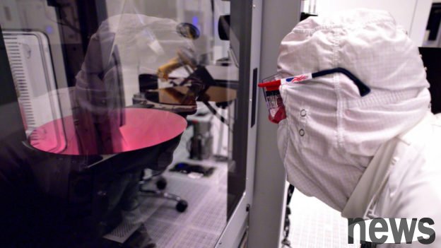
According to the market analyst's explanation of Intel's Intel 18A and 14A, it said that Intel's process maturity has not yet achieved pre-production capabilities. Because, although Intel has conducted an extremely public publicity for the Intel 18A process, its potential maturity is far from its back. Specifically, there are several major problems:
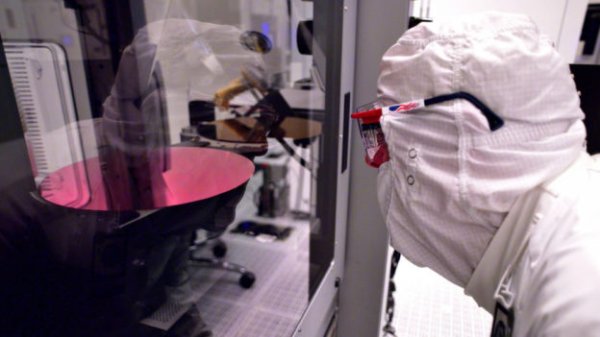
Poor yield performance: the yield rate is far below the 40-50% balance, and internal estimates are still hovering between 20-30%. Continuous technical hiccups: line width roughness, defect density, and tool stability are long-term concerns, especially after the introduction of new materials into PowerVia and RibbonFETs, these problems are even more significant. High process variations make the process variations between the wafer batches very high, indicating that the control system is immature and lacks high-capacity data recycles. The progress of the Intel 14A process is even more lagging, and has almost not reached any milestones set by customers, let alone its qualified path.In addition, based on the preparation of Intel PDK (Processing Design Kit), it is difficult for IC design companies to adopt. Because for IC design companies, Intel 18A’s PDK preparation has created a serious challenge. As of mid-2025, its PDK is still in the trial stage (many process versions are v0.9 or lower) and lacks multiple key elements. The missing elements include a fully characteristic standard cell database, a hardened SRAM/ROM translator, a certified IP block, and a LVS/DRC (Layout Verification/Design Rule Check) design kit with a certified quality, etc.
Moreover, electronic design automation (EDA) tools remain poorly related to the behavior of the actual chip, with early customer reports requiring weeks of trial cycles and lack of functionality, which undoubtedly means unacceptable design risks and progress inaccuracies for a large number of IC design customers.
In contrast, Telco has established a gold standard in the industry in terms of process and PDK maturity. As of the second quarter of 2025, N3P (3-nano reinforced version) has entered a large number of production stages, with yields exceeding 70-75%. The N2 (2nm) PDK has released v1.0+ production version, and multiple first-line customers are designing out designs. There is also complete ecological system support, including Cadence, Synopsys, Ansys, Siemens and other major manufacturers in the industry, all provide verification process support.
Finally, the most important aspect of IP ecosystem, including ARM, Imagination, Alphawave and other companies that provide certified IP cores, helping customers realize the goal of "first-time-right silicon". Taiwan Power's design enable teams provide customers with certified reference processes, migration tools and highly relevant simulation models for chips to customers around the world. This significant maturity difference is precisely why TECH is a pre-design choice for almost all cutting-edge designs.
The report pointed out that due to the above-mentioned technological maturity gap and the competition standards set by Telco, the Intel 18A/14A process will hardly have external adoption before 2028, which will also lead to serious financial consequences. First, IFS's round-foundry contract is expected to be less than US$1 billion from 2025 to 2028, far below the original cumulative contract of US$15-20 billion, continuing to drag down the already heavily pressured Intel finances.
In addition, IFS's huge costs are underway, of which annual capital expenditures will reach $1-1.2 billion by 2027. Depreciation and balance withdrawal (D&A) are expected to exceed US$4 billion per year starting from 2026. In addition, in terms of PDK, IP and EDA ecosystem expenditure, more than US$1.5 billion has been invested so far, but the relevant investment returns are extremely low. Finally, the accumulated huge amount is expected to exceed $19 billion by 2028.
In summary, unless Intel can provide PDK preparations for Intel 18A and Intel 14A with Tel water standards, as well as a high yield and pre-production capability process, it will remain the "last chosen foundry". Taiwan Electric's proven maturity with real chip verification support has won the market's trust overpriced price, which Intel has not yet obtained. Ic Design customers cannot afford to take risks on uncertified tools, unknown timetables, or non-standard processes. Therefore, by 2028, Intel's IFS will likely remain a "money pit" of high capital expenditure, low income, and almost no external customer revenue as a supplement. At the same time, NTU will further strengthen its position as the only viable partner in semiconductor production production as the leading semiconductor company.